Design Process
Project Overview

In this project, I created a logic circuit that uses three inputs to display a digit of my birthday on a seven segment display. Each input switch represents either 0 or 1 in binary, giving 8 combinations together. For each binary representation of decimal numbers 0 to 7 inclusive, the next digit of my birthday is displayed.
There were multiple constraints and limitations to this project. I had to use a cathode seven segment display, meaning segments are on when connected to 5V (HIGH) and the display itself is grounded (LOW). Additionally, I had to use 220 ohm current limiting resistors in the CAD design as the seven segment display could not handle 5V directly per LED. Also, this is a seven segment display so no fancy text can be created, only digits. Lastly, the input must be in the form of three on/off continuous switches, which means the user must know how to use binary numbers.
Truth Table
Seven segment displays (SSD) are divided into seven lights that are either on or off. They can display all digits, and some letters, but only one character at a time. In this project, each of the three input switches (X, Y, and Z) controls all segments to turn some on or some off, depending on the combination of switches. Segments are labled A to G (7 segments), and each have separate conditions under which they are on. Below is a truth table to show under which conditions each segment of the SSD will be on.
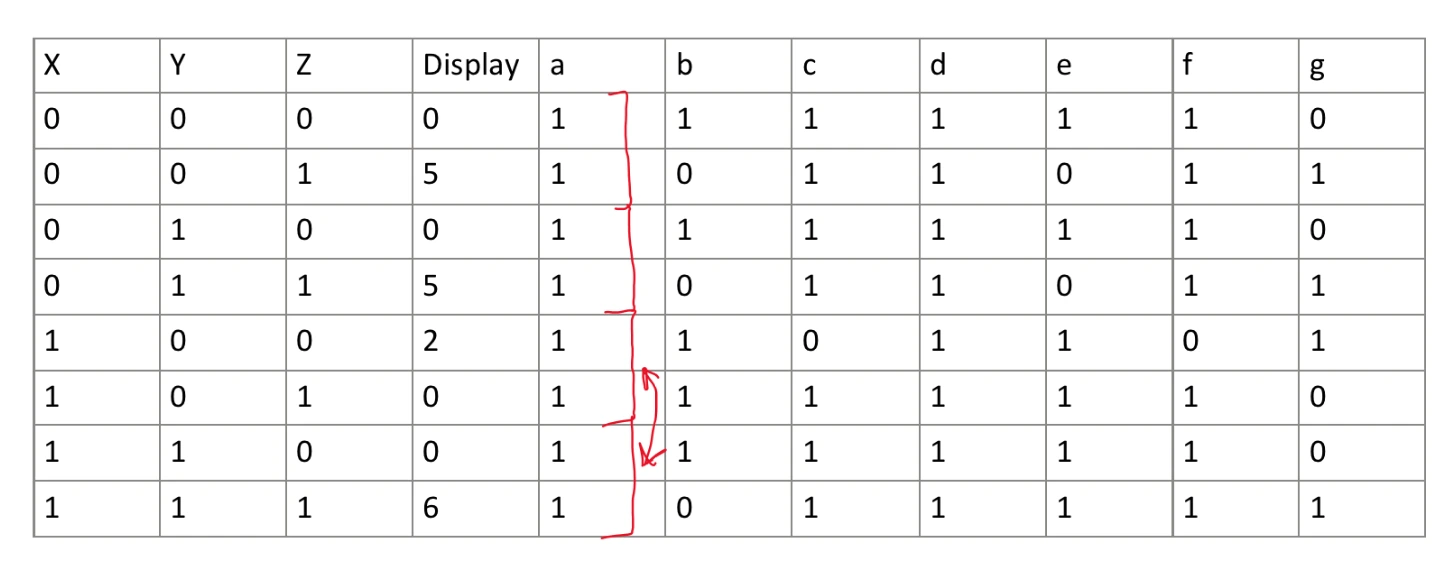
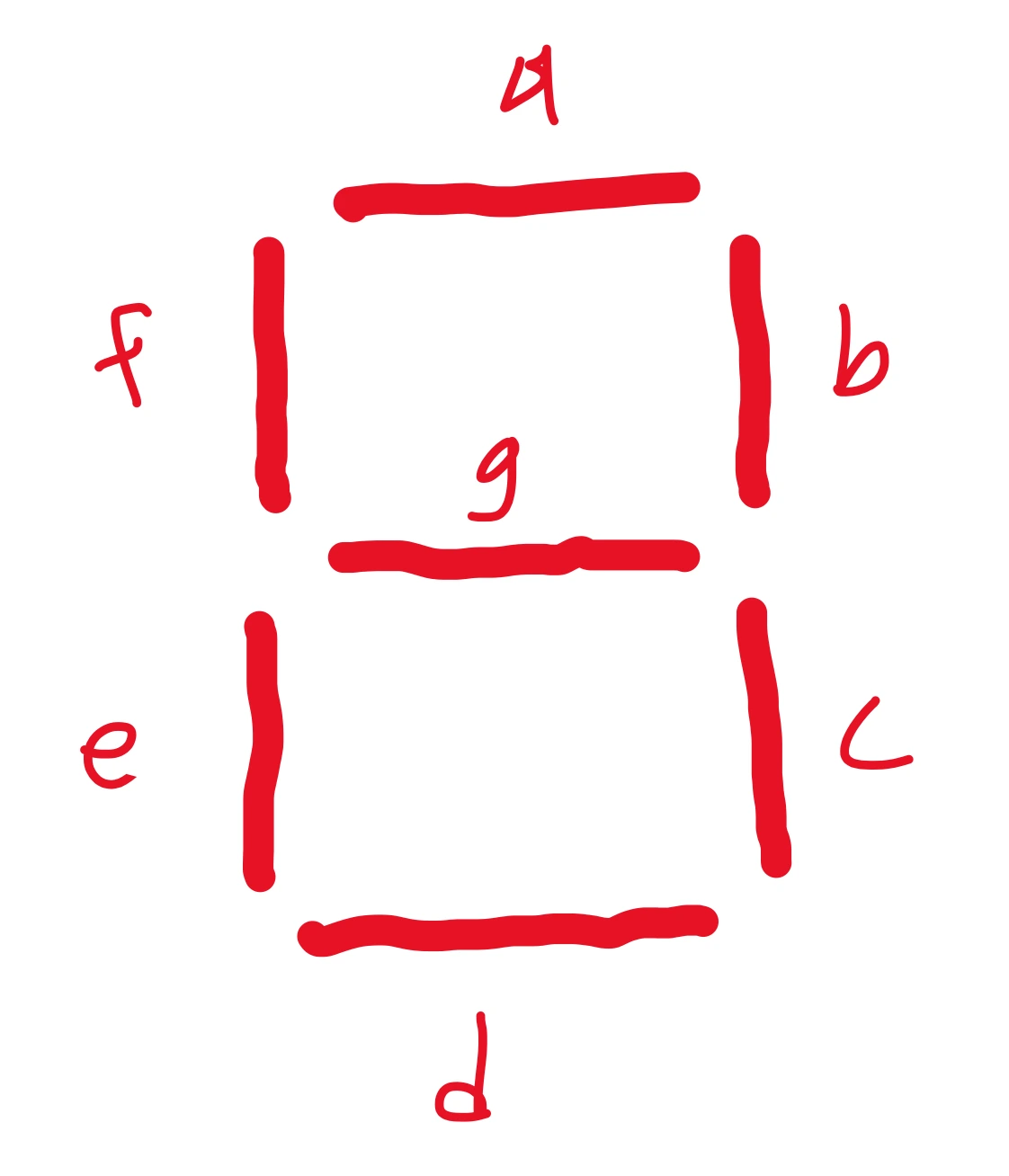
There are columns A through G, each representing a segment as seen in the other image. Inputs are the X, Y, and Z switches. For example, a zero requires that all segments are on except for G (the center segment).
K-Mapping and Simplification
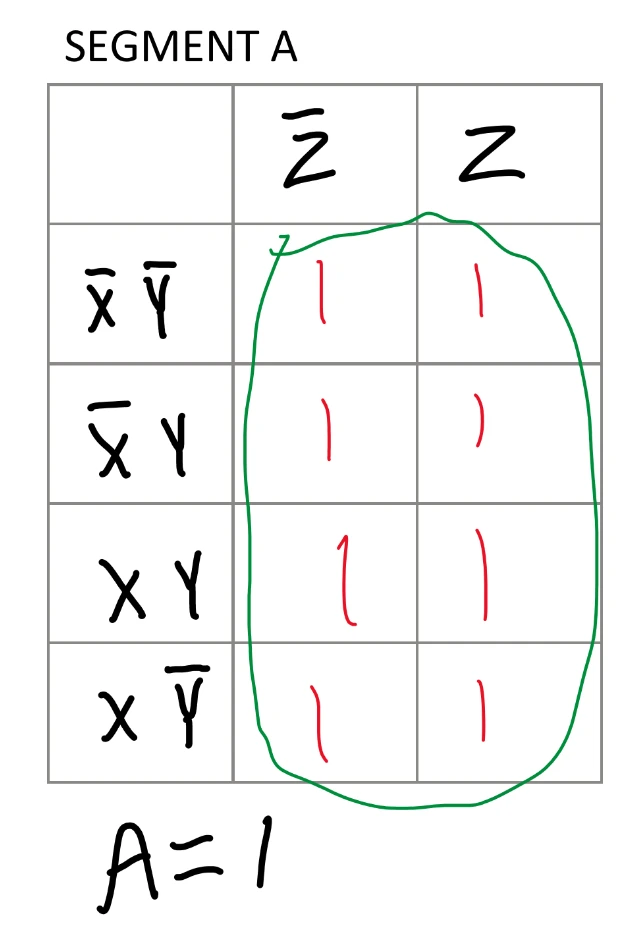
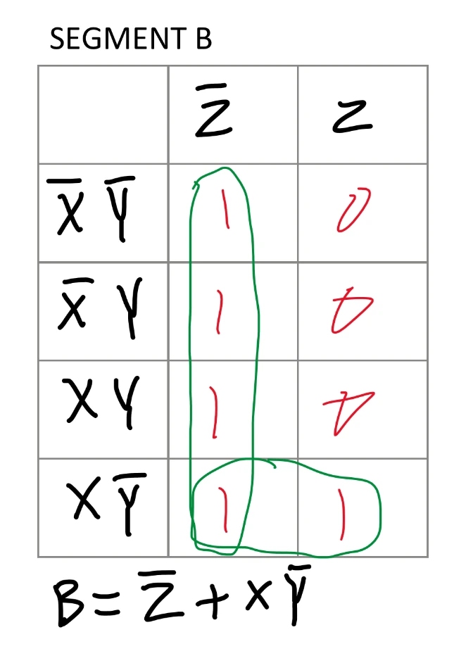
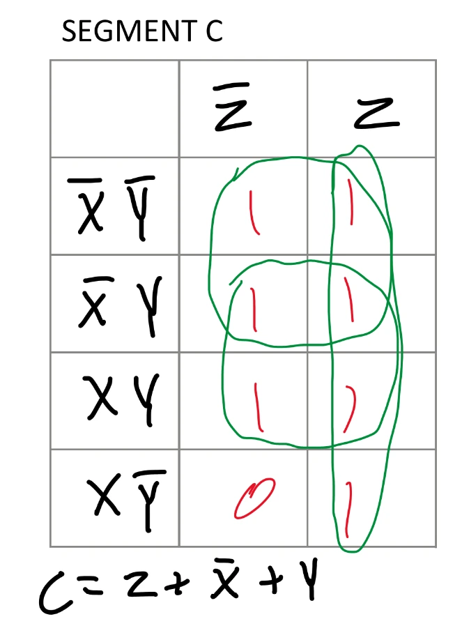
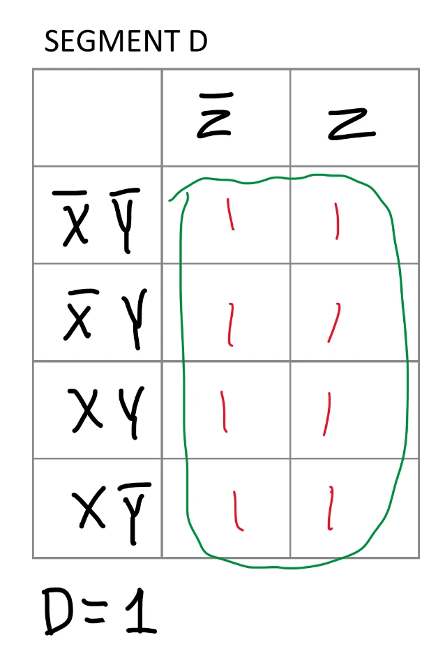
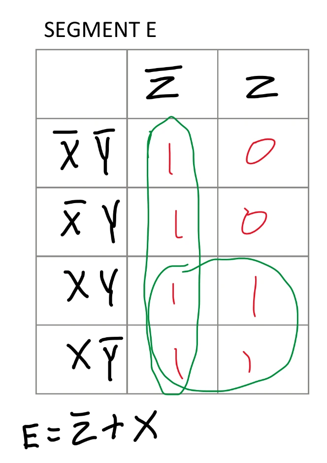
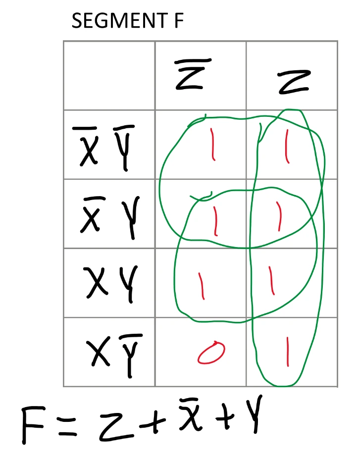
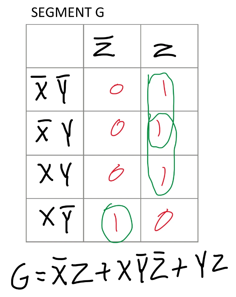
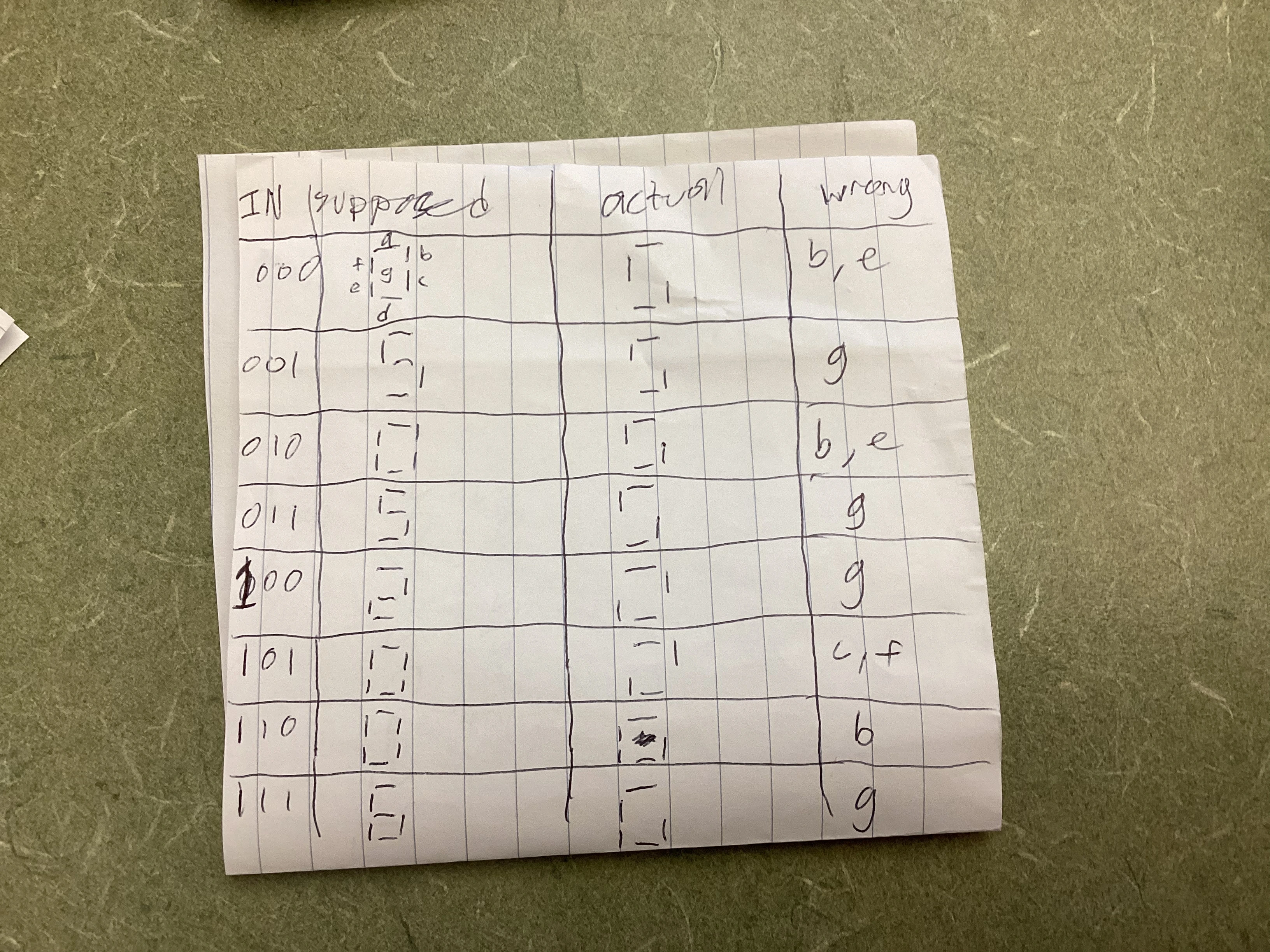
Previously in the Majority Vote project, I used boolean algebra to simplify the truth table. Boolean algebra can be time consuming and prone to errors. It is also not very visual. Instead, Karnaugh Mapping (K-Mapping) offers a visual approach to simplifying logic expressions using a table to fill in. First, a table with a rows and b columns is created, where a is 4 rows and b is 2 columns. The rows and columns are labled with every AND combination of pairs of input variables, X, Y, and Z. Next, every two rows of the truth table are grouped. After the truth table row grouping, the last two pairs of rows in the truth table are switched as shown in the truth table image. Then each pair of truth table rows is transferred to the K-map where the first truth table row goes in the first column, and the second truth table row goes in the second column. This is repeated until all pairs of truth table rows have been transferred. Now comes the grouping in the K-map. Groups can be made on the K-map in any power of two, but you start with finding larger groups (8, 4, 2, 1).
Groups are clusters of 1s in combinations of:
* 8 ones (entire K-map is full in this case)
* 4 ones
-> A square (2 rows and 2 columns)
-> A complete row or column
-> A square going over an edge and appearing again on the opposite side (like pacman)
-> A one in each corner of the K-map
* 2 ones
-> 2 adjacent 1s in a row or column
-> 2 adjacent 1s over an edge
* 1 one
-> When no other options of grouping are available, then the 1 must stay by itself in its own group.
When each table is complete, a sum of produccts is derived from which variables stay the same for each group of 1s. K-mapping automatically gives the simplest solution, which is advantageous over boolean algebra since you do not need to solve for the simplest logic equation. There are seven expressions in total, one corresponding to each segment on the seven segment display.
NI MultiSim CAD Design
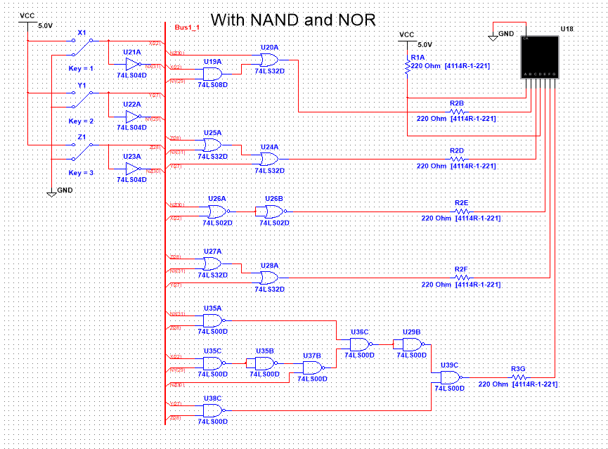
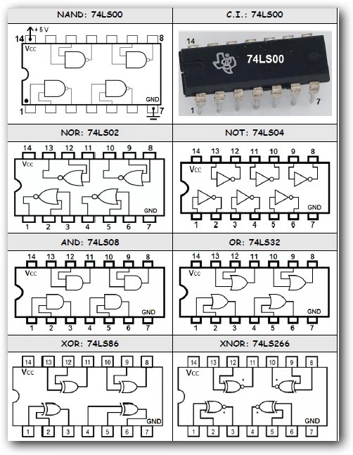
A total of 19 gates are used in this circuit. 3 74LS04 inverters, 1 74LS08 AND gate, 5 74LS32 OR gates, 2 74LS02 NOR gates, and 8 74LS00 NAND gates are used. This would require 7 ICs in total. When I created the circuit on the breadboard, I realized that segments C and F used identical logic, and was able to use one less OR gate. This brought the total down to 6 ICs consisting of 17 gates.
NAND and NOR gates are commonly referred to as "Universal Gates" since multiple NAND gates or NOR gates can be used to create any AND, OR, or NOT gate. This can be used to reduce the amount of ICs needed in some circuits by using spare NAND or NOR gates to replace other components. My circuit could not be simplified using NAND or NOR gates, so I just added them to learn how to use them. My circuit contained more ICs after adding NAND and NOR gates, but most would contain less ICs.
Back to seven segment displays (SSDs). Seven segment displays use seven LEDs to display a digit or basic letter in a human-readible format. A useful diagram is in the Truth Table section of this project page. SSDs come in two versions; common cathode and common anode. Common cathode displays take HIGH 5V as input to each LED and must always be connected to ground (GND). Common anode displays are always connected to a HIGH power source, and segments are lit when they are grounded. I used a common cathode display in this project since here HIGH means 1, which can be solved easily using K-mapping and a truth table to find out when a segment should be on. Instead, a common anode display requires you to consider when a segment is grounded, which requires grounding through boolean logic. Every LED has a 220 ohm resistor attached in the circuit to limit the current that the LED recieves. This ensures that the LED will remain in nominal conditions and will not burn-out.
Breadboarding
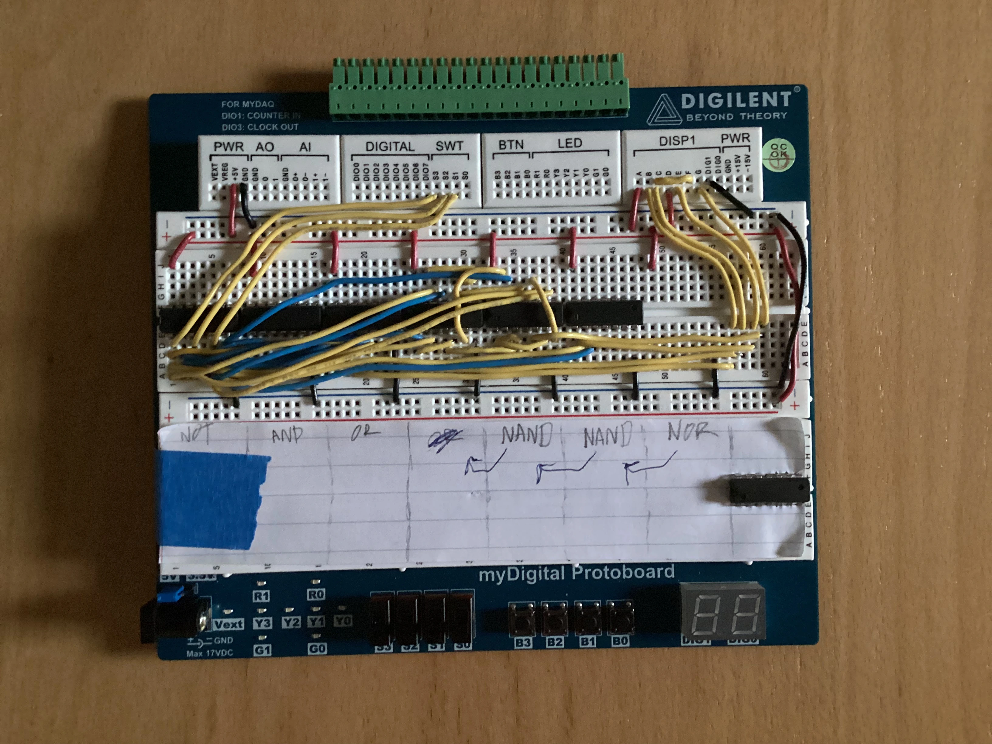
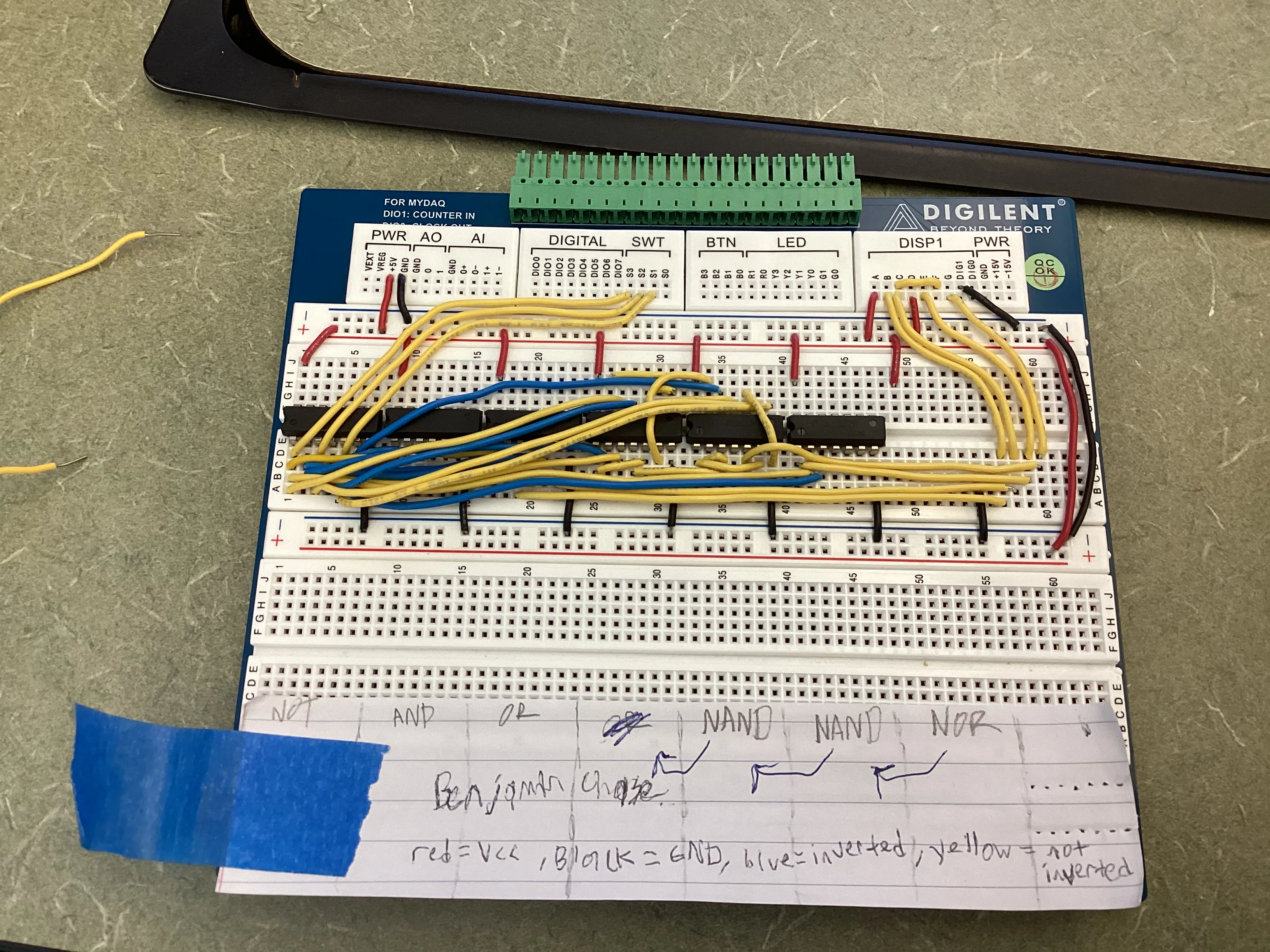
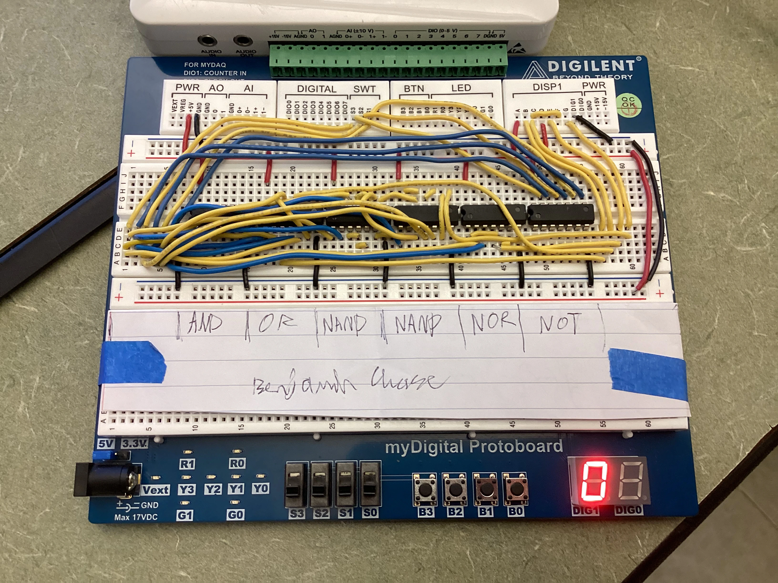
The first picture shows the first version of my circuit. It had multiple issues, such as incorrect NAND gate wiring and had all inputs directly on the inverter IC. The second picture shows an the circuit while troubleshooting. In the last image, the display is working and the inputs along with the NAND logic have been rewired.
During breadboarding the circuit, I realized that segments C and F used identical logic, so I could eliminate one OR gate. While breadboarding, I also incorrectly incorrectly connected a 74LS00 NAND gate for segment G. Generally, as seen in the IC pinout diagram above, ICs have VCC on pin 14 and GND on pin 7, along with having inputs on the left side and outputs further right. Yet 74LS02 NOR gates have these inputs and outputs reversed. I reversed the inputs and outputs since the NOR gate has reversed inputs and outputs. Knowing this, I assumed that the NAND gates would be the same, but they are not. I learned that NOR gates are the only reversed gates. To locate the issue with segment G, I used a multimeter and wire tracing to determine my mistake. While building the circuit, I cut jumper wires to custom length in order to maintain an organized layout that could easily be troubleshooted. Now all segments work perfectly.
DOB Bill of Materials
| Component | Quantity |
| 74LS04 Not/Inverter Gate | 1 |
| 74LS08 2-Input AND Gate | 1 |
| 74LS32 2-Input OR Gate | 1 |
| 74LS00 2-Input NAND Gate | 2 |
| 74LS02 2-Input NOR Gate | 1 |
| MyDigital Protoboard (SSD, breadboard, switches) | 1 |
| Wires | About 60 |
Conclusion
This project inspired me to create neat, debuggable, and more complex breadboard circuits. Along with breadboard organization, I also learned how to evaluate and simplify truth tables efficiently using Karnaugh Mapping. Before this project, I did not know how to control the output of a seven segment display. It is really just seven LEDs that can be used together to display numbers and some basic letters. If I were to redo the project, I would first find any ways to further simplify the circuit and look at all the IC pinouts while building the circuit.
Creating the Most Efficient Circuit
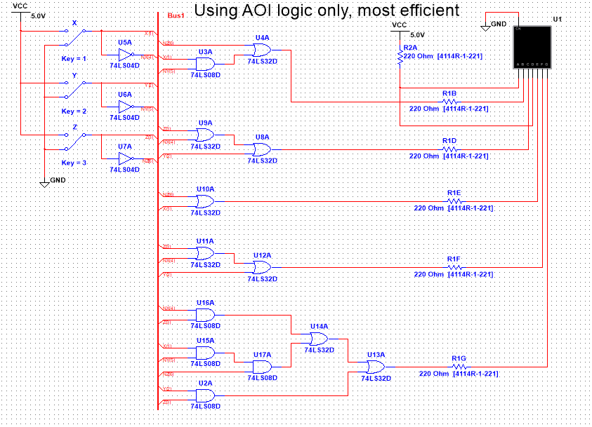
As far as I can tell, the most efficient solution of this circuit is to exclusively use AOI logic.
A screenshot is provided above from NI MultiSim.
An AOI only solution uses:
| Component | Quantity |
| 74LS04 Not/Inverter Gate | 1 |
| 74LS08 2-Input AND Gate | 5 |
| 74LS32 2-Input OR Gate | 5 (2 can be removed since C & F are the same) |
| MyDigital Protoboard (SSD, breadboard, switches) | 1 |
| Wires | About 50 |
This means that there are only 5 integrated circuits used instead of 6.